Partnership with Tescan

The chair is supported by TESCAN, originally Orsayphysics, located in Fuveau near Aix-en-Provence at the foot of Sainte-Victoire. TESCAN's goal is to support together with INSA this initiative, which aims to bring innovative developments in charged particle instruments back to the forefront of future engineer's formation. The need for increasingly versatile instruments, with the desire to enable correlative measurements between different techniques such as SIMS, FIB, etc., requires a thorough review of the optics of these instruments. This versatility must not come at the expense of sensitivity or resolution, despite increasingly demanding customer requirements for optics, such as the desire to work at low acceleration voltages for ions in order to minimise damage.
By supporting the chair, TESCAN hopes to contribute to the training of new talent in the field of charged particle optics. In line with INSA's philosophy, which emphasises the practical aspects of learning science, TESCAN will loan a latest-generation dual-beam instrument to the chair's site in the physics department of INSA Toulouse. This instrument will support the educational objectives of this teaching programme (see the page educational objective). However, this instrument, with its state-of-the-art imaging and nano-milling capabilities, will also be available to all students in Toulouse (INSA and others schools) who are not following the charged particle optics course, as part of their practical work requiring the use of an electron or ion microscope. With this tool, TESCAN will also provide our students with unique development concepts which they consider interesting for their own problematics in a win-win spirit (see the page scientific objectives)
Below is a brief history of our partner, followed by a description of the instrument shared within the framework of the chair.
- History of Orsayphysics (see also https://www.orsayphysics.com/)
The adventure began in 1989 under the leadership of Pierre Sudraud, a passionate and visionary researcher from the CNRS-Orsay in the south of Paris.
At that time, focused ion beam (FIB) technology was still in its infancy. Sudraud understood before anyone else the enormous potential of these ‘nanoscopic scalpels’ for the semiconductor industry and nanotechnology research.
The company becomes one of the world leader in particle beams. Orsay Physics technologies use ions or electrons to see, cut and build at the atomic scale. They combine home-made LMIS (Liquid Metal Ion Source) with rotationnally symmetric electrostatic lenses provided an instrument able to focus a sharp ion beam with high precision.
During the last 30 years, FIB instrumentation has become a key technology for wide fields of materials science applications, from circuit editing to Transmission Electron Microscopy (TEM) sample preparation, microstructural analysis and prototype nanomachining. Associated with a SEM (Scanning Electron Microscope), FIB instruments have become a powerful tool for nano-manipulation and nano-fabrication when coupled with micromanipulators. Equipped with a Gas Injection System (GIS) nanometric local deposition (using the GIS) can even be obtained.
In 1997, the company relocated its business from the Paris region to Provence, at the foot of the "Sainte-Victoire" (see figure 1).
Figure 1 : The TESCAN company in Fuveau (former Orsayphysics)
Today, they offer a wide range of charged particle instruments. While retaining their flagship products i.e. FIB and SEM optical columns, Orsayphysics has also recently developed a TOF-SIMS solution (time-of-flight mass spectrometers), ultra-high vacuum standalone platforms, new kinds of ion sources for FIB such as plasma sources etc.
Figure 2 reports an exhaustive list of their products, including their latest QUiiN (Quantum Ion Implanter at Nanoscale) product, which enables ions implantation with an unrivalled precision. Indeed, this last generation of ion optics instrument will be very interesting for quantum computing applications, which requires to implante ions very precisely within material structures.
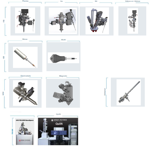
Figure 2 : The portfolio of TESCAN-Fuveau (former Orsayphysics)
- The partnership with TESCAN located in Brno (Czech republic) (see also https://tescan.com/)
Founded in 1991 by engineers from Tesla (a former state-owned company), TESCAN established itself as a specialist in scanning electron microscopes (SEM).
For more than ten years, OrsayPhysics supplied the ion columns that enabled TESCAN to transform its SEM instruments into dual beam FIB-SEM systems. Throughout this period, both companies expanded their range of increasingly high-performance instruments, following an almost identical, or at least very similar, path (see figure 3).
In 2013, the two partners decided to officially join forces to form the TESCAN ORSAY HOLDING holding company.
After the merger, the entity retained its two main production sites, one in Brno for magnetic optics based SEM and the other one in Fuveau near Aix-en-Provence for ion technologies and advanced electrostatic optics.
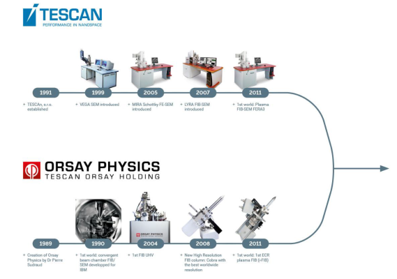
Figure 3 : From Tescan and Orsayphysics to the TESCAN-ORSAY Holding
Recently, in an effort to increase the transparency of the organization's structure, the company decided to use the name TESCAN for all its activities worldwide. The name Orsayphysics has therefore disappeared, but the heart and soul of this company remains nestled at the foot of the "Sainte Victoire", and ready to, once again, revolutionise the history of charged particle optics !
- The instrument loan to the chair : dual beam SEM-FIB
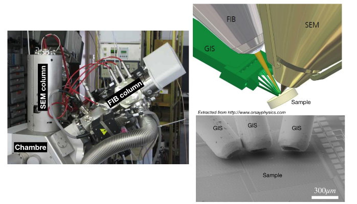
Figure 4 : The dual beam FIB-SEM instrument.
The instrument will consist of two columns in a single instrument. An ion optics based column (the FIB) and an electron optics based column (the SEM). The electron or ion beam current profile of on the sample determines the imaging resolution and micromachining precision. Generally, the smaller the beam diameter, the better the achievable resolution and milling precision.
With only ions, FIB is only a subtractive method where material is removed from the sample. To transform the system into an additive method, we add a GIS (Gas injection system) which locally delivers an organometallic gas is an efficient method to deposit material on the surface. In addition using a suitable reactive gas, it is possible to enhance the etching rate . In term of deposition process, secondary electrons generated by the primary ion beam (or, alternatively, the incident electron beam in dual-beam FIB-SEM systems) can crack hydrocarbon precursor gases, leading to local deposition of a conducting (W, Pt, C…) or insulating material (SiOx) (see figure 4). Introducing a micromanipulator in the chamber with the local deposition of material also enables sophisticated operations within the FIB system, which transform the FIB instrument in a nanofabrication unit.
The optimum system is finally obtained by gathering a FIB column, a GIS to add and remove material, a micromanipulator to move in-situ the created objects and a SEM to observe the operations at high resolution and in real time without any material removal.
This suiss knife for nanotechnology will be the instrument loan by TESCAN to the Peter Hawkes chair of charged particle optics. It will be installed inside the physics department of INSA soon.